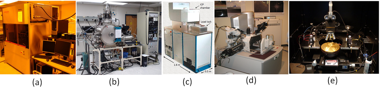
The Owen Cleanroom at OSU has campus-shared photolithography facilities and thin-film deposition systems, including direct write laser lithography [Fig (a)] and contacting photolithography to create micro- and nano- scale devices. Other commonly used fabrication facilities, such as electron beam metal sputtering [Fig (b)], thermal evaporation, and plasma-enhanced chemical vapor deposition (PECVD) system are also available. Particular, we recently acquired an Oxford Plasmalab System100 ICP380 [Fig (c)] for silicon and metal etching through the sponsorship of Murdock Foundation. In addition to that, Owen 333 hosts state-of-the-art semiconductor testing facilities, such as REL 4800 Probe station with thermal control [Fig (e)].
The Electron Microscopy Facility (EMF) provides advanced electron microscopy instrumentation services to OSU research communities. The facilities include FEI TITAN 80-200 TEM/STEM with ChemiSTEM Technology, FEI QUANTA 3D dual beam SEM-Ebeam lithography/FIB [Fig. (d)], FEI NOVA NanoSEM 230 high resolution SEM, and Leica DM 5000 computerized fluorescence optical microscope.